| 7.6.1.
Block Diagram of Voltage Unit - (БН) |
19.1 |
|
|
Real Circuit
|
|
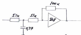
Amplifier Д8
|
 |
|
|
Note: Element designations
on the diagram (51к, 100к, Д8, 0,47 µF) are kept in original
Russian layout.
|
| GД8(p)
= |
|
; T1
= |
|
·
0.47 · 10-6 = 0.012 s |
|
|
|
Link |
|
|
 |
|
|
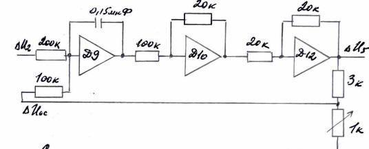
Note: Element designations
on the diagram (Д9, Д10, Д12, 0.15 µF, 200к, 100к, 20к, 3к, 1к) are
kept in original Russian layout.
|
|
The structural diagram of amplifier Д9 can be represented as
follows:
|
|
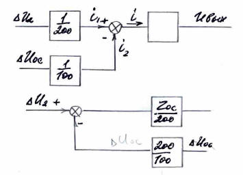
Note: Element designations
on the diagram (ΔU2, ΔUос, i1, i2,
iвых) are kept in original Russian layout.
|
|
|
= Kос
= Kп · 2 ; Kп = |
|
=
0.125 (Switch "Kп" in position 8) |
|
|